SSB and CW Transceiver
To
contact me, please use

This is a description of the transceiver I started building in
2009. It is a software defined radio receiver and transmitter on
one board. It is the heart of my current station, and I don't use
any other rig at my shack. Detlef Rohde DL7IY and Gunter Richter
DL7LA published an article describing the design in the August 2010
issue of Funk Amateur (in German). My article appeared in the
January/February 2011 issue of QEX.
New Hardware and Software
The QEX article describing my hardware design was published in the
January/February 2011 issue, and since then a number of people have been improving my design and adding
features. The new design is called the HiQSDR. They now
have PC boards and assembled units available. I am working to
improve the Quisk software for use with their hardware. See
http://www.hiqsdr.org
technologie2000.de
http://dl2stg.de/stefan/hiqsdr/index.html
http://groups.yahoo.com/neo/groups/n2adr-sdr
New FPGA Firmware is Available
You
should use the most recent firmware available. But if you already
have firmware installed, you do not need to update unless you need the
new features.
David Fainitski, N7DDC, has published new firmware for the HiQSDR. See
the Quisk group with the topic "HiqSDR new firmware ported from Odyssey" by N7DDC
from October 2020.
Stefan, DL2STG, publishes FPGA firmware that offers advanced
features. These versions still work with Quisk. His FPGA
firmware can return blocks of raw samples so you can perform an FFT of
the whole 60 megahertz bandwidth; and it offers higher sample rates of
1920 ksps at 16 bits, and 3840 ksps at 8 bits. The most recent
version as of February 2013 is FPGA-1.3-sg2, but look for the most
recent version at http://dl2stg.de/stefan/hiqsdr/fpga.html.
These are my original versions written for Quisk and the HiQSDR:
April 2013 firmware version 1.4 is now available.
This version allows you to change the IP address of the hardware from
the PC instead of using the address programmed into the firmware.
It also changes FPGA pin 56 to be an output pin; high for normal, and
low for full duplex (FDX) operation.
A new firmware version 1.3 is now available.
This version fixes a problem with spectrum flatness when sampling at
960 ksps, and adds the special features used by the Quisk VNA
program. The VNA program "quisk_vna.py" enables the hardware to
be used as a vector network analyzer, and it requires this firmware or
above.
A new firmware version 1.2 is now available. This version includes support for wider transmission bandwidths up to 22 kHz for wider FM and for DRM. There
is also a new "Qs" command that returns the hardware status as the same
string used by the "St" command. There is no need to upgrade
unless you need to
transmit FM, or you wish to query the hardware with the "Qs" command (for example by Hamlib).
A new firmware version 1.1 is now available.
It works fine with the original hardware, but also supports the extra
features of the HiQSDR. Specifically it
supports the X1 connector FPGA pins 69, 68, 65, 64 (band in use) ;
preamp pin 63; transmit LED pin 57; the attenuator pins 84, 83, 82, 81,
80; and the antenna switch pin 41. There is also a new PTT (push
to talk) input pin 176 that is used instead of the key input (pin 177)
for SSB. Be sure to use this pin for SSB instead of the key pin
if you use the new firmware. This new firmware requires Quisk
version 3.5.5 or later. For the original hardware you must set
use_rx_udp to 1 in your config file, and for the HiQSDR you must set it
to 2.
The original firmware was version 1.0. It still works fine with
newer versions of Quisk. There is no need to upgrade your
firmware unless you need the new features. Note that the firmware
version you are using appears on the config screen. Be sure to set use_rx_udp to 1.
Original N2ADR Hardware
My 2010 software defined radio (SDR) project is an SSB and CW
receiver and exciter on
the same board. It is the successor to my SSB exciter from
2007. It improves on the 2007 hardware by using a 10/100 Ethernet
controller, eliminating the microcontroller bottleneck, and including a
receiver on the same board. You should still read my May/June 2008 QEX article
for background.
The hardware design is very straight forward. A block diagram is
available here. In the center is
an
Altera FPGA and its program storage chip. This is connected to
everything else:
- An 10/100 full duplex Ethernet controller and its RJ-11
jack. All communication is over UDP packets on Ethernet.
The FPGA program supports Ping, ARP, Tx samples, Rx samples, tuning and
status.
- An analog to digital converter (ADC) and its preamp for receive.
- A digital to analog converter (DAC) for transmit.
- Another 8-bit DAC to control the transmit output level.
- A low jitter 122.88 MHz clock.
The major parts were all purchased from Digikey and are a follows:
- The FPGA is an Altera EP3C25Q240C8N, 240 pins, programmed by an
EPCS16SI8N.
- The Ethernet controller is a LAN9115, and runs full duplex at 10
or 100 mbps.
- The Ethernet jack is a Stewart SI-50170-F, Digikey part number
380-1103-ND.
- The clock is a Crystek 122.88 MHz CVHD-950-122.880.
- The receive ADC is a 125 MHz 14-bit Texas Instruments ADS5500IPAP
in 64-TQFP.
- The ADC preamp is a Linear Technology LTC6405.
- The transmit DAC is an Analog Devices 14-bit AD9744.
- The transmit level control DAC is an Analog Devices AD7801.
- The box is a cap cover L190, size 5X7X2 inches.
A few people have expressed interest, so I am providing the design
files as an open source project. Please note that THERE ARE NO
WARRANTIES. I have a full time job, and can supply only a little
support to interested parties.
If you want to play with software defined radio and need a place to
start, feel free to study or build this project. I suggest you
mount just the FPGA first, and test it with the usual LED blink
program. Then mount the Ethernet controller and test it with
Ping.
Then you can mount the more expensive ADC or DAC or both.
This project is just a transceiver. To make a complete station
you need amplifiers and filters. A block diagram and description
of the rest of my station is here.
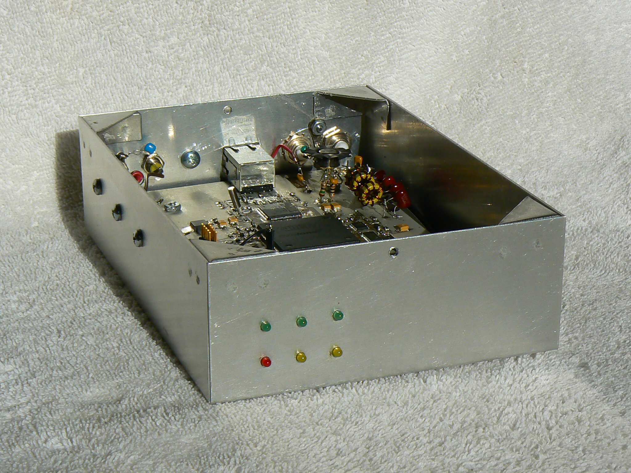
Photos
Here is a screenshot of Quisk running
with the new hardware. It shows the whole 40 meter amateur band
sampled at 480,000 samples per second. Here is a photo of the hardware and a photo of the PC board.
PC Board
The PC board design is finished and was done with Eagle. The
design files as of December 2009 are in eagleboard.zip.
This
is
a
rev 2 board and there are some problems you may want to fix
if you are going to make more boards. The TO-220 voltage
regulators are not on the board, they are mounted on the box, and the
DAC output amplifier is added to a bare space on the PC board.
The schematic is here.
The board is two-layer because multi-layer boards are very expensive in
quantity one. But this creates problems with noise. To
reduce noise, I left as much copper as possible on both sides. As
a result, there are a number of jumpers that must be added. The
board should really have at least four layers.
To add jumpers to the back of the board, start the Eagle PCB software,
and look for yellow "air wires". These are the jumpers you
need. You can also use the highlight feature on a through-hole
pad to see which other pads light up. All jumpers have pads.
You must solder the pad on the bottom of the ADC preamp to
ground. First mount the preamp. Then turn the board over,
and note that there is a plated-through hole on the board at the center
of the preamp. Add a bit of flux to the pad using this
hole. Then use a narrow soldering iron tip to wet the pad with
solder. Let the solder flow onto the hot pad, and then quickly
fill the hole with solder. Finish by flowing the solder over onto
the ground plane. Work quickly, or you might disolve the plating
on the hole.
The remaining problems are:
- The pads for the Schottky diodes and the ferrite chips should be
larger.
- There should be a bleeder resistor for the 2.5 volt regulator
(minimum current spec).
- The holes for the 2X5 programming pin header are too big.
- There should be more space around the through-hole pads.
- The LED eight lamp array is too bright; increase the resistor
value.
- Perhaps put some of the voltage regulators on board instead of on
chassis.
The input power is 6.0 volts, and I mounted TO-220 regulators on the
chassis for 5.0, 3.3 and 1.2 volts. The 2.5 volt regulator is on
the board.
I built the DAC low pass filter and preamp on the board using "ugly"
construction (there are no board traces). The alternative is to
run the DAC output directly to the BNC. The board has a lot of
empty space for this type of modification.
Software
The transceiver is controlled by my Quisk
software. If you do not want to use Quisk, just attach your
own software. Audio samples from the receiver are pairs of 24-bit
I/Q samples starting at UDP data position 2 (Ethernet position
44). The first byte of UDP data is a sequence number that
you can ignore, or use to check for errors. The second status
byte carries the key up/down state and an ADC overrange bit. To
transmit, send two
8-bit zeros followed by 16-bit I/Q audio samples to UDP port 0xBC79 at
a 48 kHz rate. For control, check the simple UDP code in
quisk_hardware_n2adr.py.
The FPGA software is written in Verilog for the Altera free Web Edition
development environment. You will need a programming cable to
connect the 2X5 header to your PC. I use the Terasic P0302 USB
cable (Digikey P0302-ND) instead of the more expensive Altera cable.
The FPGA project files are now final (or as final as homebrew projects
ever get). The decimation from the 122.880 megahertz clock
is 8 times the decimation specified in the config file (2 to 40) times
8. That results in a final sample rate of 48000 to 960000 samples
per second. At 960000 sps and 48-bit samples, the Ethernet
bandwidth is 46 megabits per second plus 1.5 mbs for transmit plus
overhead, or about half the available 100 mbs Ethernet bandwidth.
Status
2013 November: Continuing work on HiQSDR and Quisk.
2011 January: The QEX article was published.
2010 May: The hardware and software are finished and work
well. I submitted an article describing this project to QEX.
2010 April: Thanks to an email from Jeff Millar, WA1HCO, I now
understand the high noise figure. He calculated the noise figure
of the ADC alone to be 30 dB. The preamp gain is not sufficient
to dominate the noise figure, and using the usual formula F = F1 + (F2
- 1) / G1 gives the net noise figure I observe. I do not want
more preamp gain, as that would degrade the dynamic range. I have
an additional preamp external to the transceiver that I can switch in
for 20 meters and up.
2010 April: The FPGA software is almost finished. I added
the ability to specify the decimation rate in the Quisk config
file. SSB transmit and receive both work.
2010 January: The receiver noise figure is 24 dB. Although this
is not bad, the preamp noise is dominant, and I was expecting a noise
figure closer to the preamp noise figure of 7.5 dB. I do not
understand why the noise figure is 24 dB. The transmitter audio
is good. The output from a low pass filter connected to the DAC
transformer is 2.2 dBm at 1.9 MHz, 1.6 dBm at 14.2 MHz, and 0.5 dBm at
30 MHz. The 20 ma peak (10 ma after the transformer) from the DAC
to parallel 180 and 50 ohm loads would give 1.85 dBm in the 50 ohm
load. This goes to a 2N5109 amp with 15 dB gain, but the IMD is
about 35 dB below one tone. At this power level, lower IMD
is expected, so I plan to reduce the gain.
2010 January: The FPGA software now generates both CW and
SSB. Two-tone output is generated in audio and sent as SSB, and
looks good.
2009 December: This project is not finished and currently is
under
development.
The board is done and all the parts are mounted. Receive mostly
seems
to work, although the noise level is higher than it should be.
The
transmitter generates sin waves but not SSB.